Electronics today… they look simple from the outside. A phone, a laptop, even a small device. But inside? It’s all about the PCB. And when you hear the term “Veda PCB”, it usually connects to companies or services that specialize in PCB design, layout, and engineering solutions.
Let’s break it down in a real, practical way — no confusion, no heavy jargon.
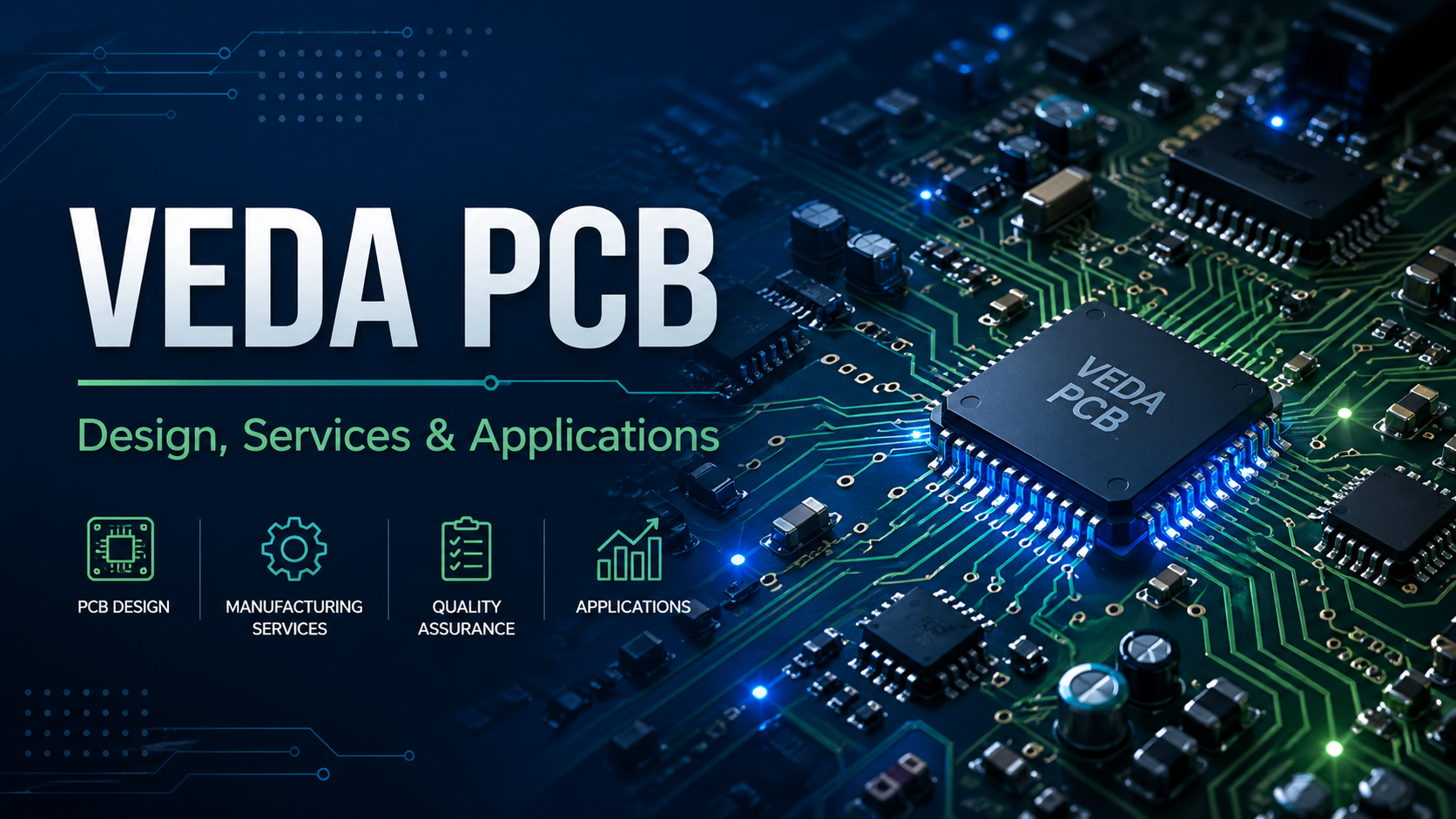
What is Veda PCB?
“Veda PCB” isn’t a single fixed product. It’s more like a term linked to companies or services (like Veda circuit solutions or VEDA engineering firms) that provide PCB design and development.
In simple words:
- PCB = Printed Circuit Board
- It is the base where electronic components are connected
- Every device — from mobile to AC — depends on it
And “Veda PCB” usually refers to:
- PCB design services
- PCB layout engineering
- High-speed or custom board development
- Electronics consulting
Some Veda-based companies focus on analog, digital, and mixed PCB design, including advanced engineering solutions
How PCB Works (Simple Explanation)
A PCB may look like a flat green board… but it’s doing serious work.
Here’s how it works:
- Copper tracks act like roads for electricity
- Components (resistors, chips, capacitors) sit on the board
- Signals travel through designed pathways
- Everything connects in a controlled way
Basic Flow of a PCB System
| Stage | What Happens |
|---|---|
| Input | Power enters the board |
| Processing | Signals move through components |
| Output | Device performs function |
Without PCB… your device is basically useless.
What Makes “Veda PCB” Different?
Not every PCB service is equal. This is where Veda-type PCB services stand out.
They usually focus on:
- Precision design
- High-performance boards
- Industry-level projects
- Real-world applications
Key Features of Veda PCB Services
- Custom PCB Layouts – tailored for specific devices
- High-Speed Design – for advanced electronics
- Power Supply Boards – stable energy management
- Control Systems – used in automation
- Testing & Validation – ensures reliability
And yeah… this is where beginners often get confused.
It’s not just about drawing lines on a board — it’s about engineering logic + performance + reliability.
Types of PCB Designs Used in Veda PCB Work
Different projects need different boards.
Here are the common types:
1. Single Layer PCB
- Simple and low cost
- Used in basic electronics
2. Double Layer PCB
- More connections
- Better performance
3. Multi-Layer PCB
- Complex circuits
- Used in computers and mobiles
4. High-Speed PCB
- Designed for fast signal transfer
- Requires expert-level layout
Real Applications of Veda PCB
This is where things get interesting…
PCB is everywhere. Literally.
Common Use Cases
- Smartphones
- Laptops & computers
- Industrial machines
- Medical devices
- Automotive systems
- Home appliances
Even your air conditioner depends on PCB for power control and automation
Veda PCB Design Process (Step-by-Step)
Now let’s talk real workflow. This is how a typical PCB project goes.
Step 1: Requirement Analysis
- What device are you building?
- What power and signals are needed?
Step 2: Schematic Design
- Logical circuit is created
- Components are selected
Step 3: PCB Layout
- Components placed on board
- Routing (connections) is done
Step 4: Simulation & Testing
- Check for errors
- Improve performance
Step 5: Manufacturing
- Board is produced
Step 6: Assembly (PCBA)
- Components are added to PCB
PCB vs PCBA (Important Difference)
Many people mix this up…
| Term | Meaning |
|---|---|
| PCB | Empty board with tracks |
| PCBA | Fully assembled board |
So when someone says “Veda PCB”… sometimes they actually mean full PCBA services.
Benefits of Using Veda PCB Services
Let’s be honest — why choose a specialized service?
Major Advantages
- High accuracy design
- Better performance
- Reduced signal noise
- Compact design
- Reliable long-term use
And one more thing…
A well-designed PCB can last for years without issues.
Common Mistakes Beginners Make
This part matters — especially if you’re into electronics or business.
Mistakes to Avoid
- Ignoring heat management
- Poor routing design
- Wrong component placement
- Not testing before manufacturing
- Choosing cheap low-quality vendors
These mistakes? They can destroy your entire project.
Veda PCB in Industry (Why It Matters)
Modern industries depend heavily on PCB.
Companies working in PCB design (like Veda-type firms) often handle:
- Semiconductor projects
- Embedded systems
- VLSI-related designs
- Industrial automation boards
Some organizations even provide training in VLSI and embedded systems alongside PCB design, showing how important this field is in electronics engineering
Future of Veda PCB
The future looks strong… and fast.
Trends to Watch
- AI-based PCB design
- Miniaturization (smaller boards)
- High-speed communication boards
- IoT device integration
- Flexible PCBs
And yeah — demand is only increasing.
Every smart device needs a smarter PCB.
FAQs About Veda PCB
What is Veda PCB?
It refers to PCB design and engineering services offered by Veda-related companies or professionals.
Is Veda PCB a company or a product?
It can be both — usually a company or service provider working in PCB design.
What does PCB stand for?
Printed Circuit Board — the base of all electronic devices.
Is PCB design a good career?
Yes, especially in electronics, embedded systems, and VLSI fields.
What tools are used in PCB design?
Common tools include Altium Designer, Eagle, KiCad, and OrCAD.
Conclusion
So… here’s the simple truth.
“Veda PCB” isn’t just a keyword — it represents a whole ecosystem of PCB design, engineering, and real-world electronics development.
From small circuits to advanced systems — everything depends on PCB. And services like Veda help turn ideas into working hardware.
If you’re building a tech business, doing freelancing, or even learning electronics… understanding PCB is not optional anymore.
It’s the foundation.